

Cutting Carbon in Wafer Fabs: The Truth About IR Heating
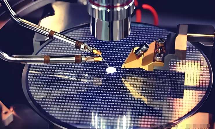
Let’s be honest—semiconductor tools are absolute power hogs. If you look at the carbon footprint of a wafer fab, the biggest waste usually happens in the thermal budget. For years, we’ve just heated up the entire vacuum chamber like a giant oven, which is basically like heating your whole house just to warm up a slice of pizza. Switching to targeted infrared (IR) lamp systems changes that. Instead of warming everything, you put the heat exactly where the wafer needs it. Why IR actually works It comes down to short-wave IR lamps. These things are fast. Really fast. They hit the wafer surface and react almost the second you tweak the power. Since you aren’t relying on convection, you get a direct energy transfer. No more sitting around and wasting kilowatts while you wait for a chamber to hit a set point. Your ramp-up times just vanish. The catch (because there’s always a catch) Here’s the thing: high-wattage IR lamps pack a serious punch. That heat density is great for the wafer, but it’s a nightmare for the tool’s chassis. If you push a ton of power through those lamps, the surrounding hardware takes a beating. You have to be obsessive about your cooling manifolds and heat exchangers. If your cooling loop can’t dump that ambient heat, your sensors start to drift. And once that happens, your process uniformity goes right out the window. Making the “Green Factory” thing actually happen When you move to IR, you stop fighting physics and start using it. By narrowing the emission spectrum to match what the wafer actually absorbs, you stop wasting energy on the tool walls. We see this most during bake-out and curing cycles. Plus, you get faster throughput and lower kWh per chip. It’s just common sense applied to the shop floor. Less waste, more wafers, and a much smaller footprint.