
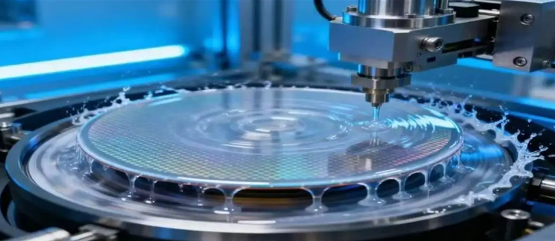
On the fab floor, furnace thermal drift isn’t just a number on a display. It shows up as critical dimension shifts and messed-up doping profiles across the wafer. One hot zone that’s off, and you’re chasing yield loss through photoresist bake variability and film stress that never quite lines up the same way twice.
What matters, technically
Our LPCVD furnace heating element is built around repeatable temperature control, aiming for wafer-level thermal uniformity within ±0.1°C across the load. The hot-zone design keeps gradients down and locks in the thermal budget your process recipe depends on. Quartz and engineered ceramic interfaces keep particle generation at zero, so you can run cleanroom Class 1–100 without adding contamination risk. Fast response and stable steady-state output give you tighter bake margins in photoresist processing—soft bake and hard bake profiles stay consistent, run after run.
Why it holds up in production
In wafer manufacturing, lithography and film deposition are sensitive to tiny temperature excursions. This element keeps the furnace profile predictable, so critical dimensions hold, overlay improves, and rework drops. For semiconductor packaging lines, the same stability cuts thermal-induced warpage and improves bond quality. Energy use stays optimized through efficient heating and minimal overshoot, so operating cost comes down without slowing cycle time. Reliability is baked in—units run 24/7, and maintenance intervals stay predictable.
What you need to get right
Installation comes down to exact mechanical alignment and verified electrical terminations. If the mounting doesn’t match, you’ll introduce localized stress and drift. Make sure your furnace tooling, connector type, and voltage class are confirmed before integration. The element performs best when you pair it with calibrated temperature monitoring and routine hot-zone inspections—schedule those checks if you want to keep the stated uniformity and particle performance.